Flexible Printed Circuit Board (FPCB) are offered in a number of layer configurations ranging from Single Sided, Double Sided THP (2 layer), to 8 layer (multilayer) stack builds. Two types of laminate materials are offered, these being Polyimide (Kapton) and Polyester. Both are available in varying thickness, Polyimide being the more popular due to its superior mechanical stability over large temperature ranges.
Generally the one material type is used for both substrate and the insulation layers
(if applicable). The outside conductors (typically copper) can be covered in conventional solder mask or covered with a Polyimide/polyester insulator layer.
Due to the diversity of applications, a large range of options exist relating to material thickness, conductor types and thickness, as well as stiffening options. These options exist to allow designs to best fit the application at the most cost effective price.
Stiffeners are as the name implies, a mechanism to stiffen the flexible PCB (usually only on part of the area) to ensure a higher level of rigidity at the stiffened location. This may be needed for a number of reasons such as mounting/fixing or to ensure a reduced amount of flexing at a location where SMT components are mounted. Heat dissipation and thermal control would be a reason why a metallic stiffener is used. A number of different materials are offered for this process as per the Manufacturing capability.
Most commonly stiffeners are either FR4 laminate or polyimide and are bonded using an epoxy adhesive. Impedance control and shielding also lends itself well to this technology, not only for the design of multi-layer boards which support components, but for flex boards which act as cable assemblies.

Type S
Single Side
The Single Sided structure is a basic structure with the Land formed only on one side. It is mainly applied for the reciprocating motion on the pick-up section of ODD products or 3D wiring for the small home appliances using the bending among the FPCB features.
Application
- 3D wiring for Camcorder and CDRW.
- Drive section of CDRW Pick-up
- Drive section of CDRW Deck
- Drive section of Inkjet Printer Head
- Grounding for electro-magnetic
shielding of mobile phones
- Simple connecting circuit among units
of various products

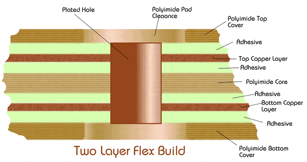
Type D
Double Side
Double Side, the copper sheets are bonded to the top and bottom of the PI films. Since the land, which is the welded part, can be formed at the top and bottom on this structure, the density of the components can be improved when compared to other structures of the same size.
Application
- LCD and TFT-LCD Fusion
- Mobile Phone Keypad, Side Key
- Higher density circuits than S/S
- Mounting components to FPC
Type A
.jpg)
Type DA
Double Access
Dobule Access Type products, the copper sheets are raw materials without the PI films.
While these products are similar to D/S because the upper and lower sides of Coverlay are bonded, the top side of one copper sheet is bonded to the Coverlay and so the pattern is formed. Then, the bottom side is bonded to the Coverlay.
Application
- Folder Type Mobile Phone
.jpg)
Type M
Multilayer
As the home appliances and communication devices become more compact and have higher functionality, the products tend to be multi-layered for mounting more circuits and components on the same sized product.
Application
- Color, Folder Type Mobile Phone
- High Density Circuit
.jpg)
This characteristic cannot be reproduced economically, if at all, using conventional wiring techniques. The tight mechanical manufacturing tolerances translate to the impedance also being controlled to a tight level.
Flexible circuit boards may require a tight radius fold which holds its shape in a relaxed position. The application of this fold is called forming and is a standard option we offer. Customers need to however take into consideration that this process may be better implemented after loading of the PCB to avoid problems with handling and compatibility with pick and place machines.
Flexible PCBs normally have a complex shape. Unlike rigid boards which can be routed and/or V-Grooved, these options are not available for flexible PCBs. The circuits can only be cut out using a punch tool or a laser cutter.
There are two types of punch tools available, the first is a Steel Rule Die (SRD). The second is a Punch & Die tool.
The SRD is elatively low cost to manufacture as it consists of sharp steel cutting blades embedded into a soft wood base. The tool has a short cycle life and as such is suited to samples and small production run quantities.
The Punch and Die tool on the other hand is a high tolerance, high precision, long life tool and is the only suitable option for production quantities. The tool is first designed using CAD and then machined on CNC mills using tool grade steel. The cost of the tool varies greatly and is dependant on the size and complexity of design.
Laser cutting has very high precision, however it is a relatively slow process, hence making it only really suitable for prototypes or small production volumes. The PCB Company P/L offer all three cut out options and will advise customer as to the best option given the customer's requirements.